
| Back to the JOYCE activities |
|
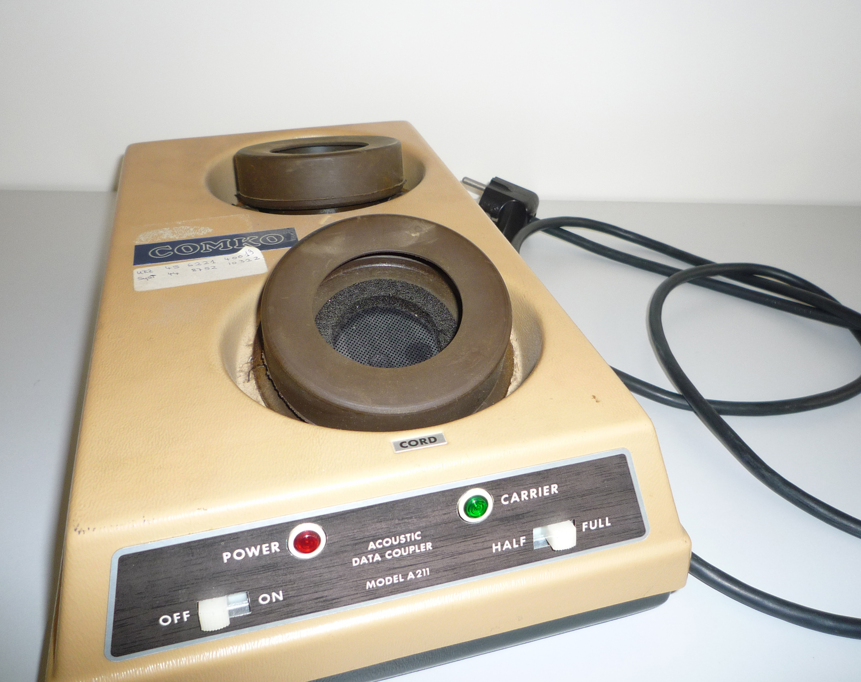
| Werner Cirsovius well known by his firmware articles in the NEWS 2+3/87 describes the serial interface and its programming here. As distinguished from other listings – mainly written in Pascal and not usable for everyone – neither the source assembler code nor the basic loader will be released on disk but the result of this article: the public domain tool KERMIT especially customized for the JOYCE by Werner! |
| BIT | 7 | 6 | 5 | 4 | 3 | 2 | 1 | 0 |
| SC1 | SC0 | RL1 | RL0 | M2 | M1 | M0 | BCD |
| F = fCPU / (32*BAUD) |
	timer   equ     0e7h
        baud0   equ     0e4h
        word    equ     0011$0110b
        value   equ     417

doit:   mvi     a,wrd
        out     timer
        mvi     a,low value
        out     baud0
        mvi     a,high value
        out     baud0
        ret
|
1000 baud=300 1010 value=4000000!/(32*baud) 1020 OUT &HE7,&H36 1030 OUT &HE4,value MOD 256 1040 OUT &HE4,value\256 1050 RETURN |
program BaudRate;
const
  Word   = $36;
  Baud0  = $E4;
  Value  = 417;

procedure bd_set(Word, Baud0,
                 Value : integer);
const
  Timer  = $E7;
begin
  port[Timer] := Word;
  port[Baud0] := lo(Value);
  port[Baud0] := hi(Value);
end;

begin
  bd_set(Word, Baud0, Value);
end.
|
        CALL    USERF
        DW      XBIOS_FUN
The XBIOS functions may be divided into:
| XBIOS_FUN: | 00B6H | |
| Subfunction: | Set UART values | |
| Register: | Accu | Selected mode |
| 00H: No handshake | ||
| FFH: Handshake | ||
| D | Number of stop bits | |
| 0 : 1 stop bit | ||
| 1 : 1,5 stop bits | ||
| 2 : 2 stop bits | ||
| E | Parity | |
| 0 : None | ||
| 1 : Odd | ||
| 2 : Even | ||
| H | Number of receiver data bits | |
| L | Number of transmitter data bits (5, 6, 7 or 8) | |
| Subfunction: | Set or reset UART bits DTR and RTS | |
| Register: | Accu | 7DH RTS on |
| 7EH RTS off | ||
| 7FH DTR on | ||
| 80H DTR ofd | ||
| XBIOS_FUN: | 00B9H |
| Register: | H coded receiver Baud rate |
| L coded transmitter Baud rate |
| Code: | 0: | — | 8: | 1200 Bd |
| 1: | 50 Bd | 9: | 1800 Bd | |
| 2: | 75 Bd | 10: | 2400 Bd | |
| 3: | 110 Bd | 11: | 3600 Bd | |
| 4: | 134,5 Bd | 12: | 4800 Bd | |
| 5: | 150 Bd | 13: | 7200 Bd | |
| 6: | 300 Bd | 14: | 9600 Bd | |
| 7: | 600 Bd | 15: | 19200 Bd |
| XBIOS_FUN: | 00BCH | |
| After calling this functions the registers hold the following values: | ||
| Accu | 00H: No handshake | |
| FFH: Handshake | ||
| B | Coded receiver Baud rate | |
| C | Coded transmitter Baud rate | |
| D | Stop bits (see above) | |
| E | Parity (see above) | |
| H | Number of receiver data bits (see above) | |
| L | Number of transmitter data bits (see above) | |
        CALL USERF      ;Read UART setting
        DW   00BCH
        MOV  H,B        ;Let receiver as is
        MVI  L,6        ;Transmitter 300 Baud
        CALL USERF      ;Set Baud rate
        DW   00B9H
One final question has to be solved − how to program the subroutine "USERF".
Concerning this the BIOS vector of function 30 must be initalized at the beginning of a program
INIT:   LHLD 1          ;BIOS base address
        LXI  B,3*(30-1) ;Load offset
        DAD  B          ;Calculate vector
        SHLD USERF+1    ;Save as jump address
        RET
USERF:  JMP  $-$        ;Jump to BIOS function 30
| 7 | 6 | 5 | 4 | 3 | 2 | 1 | 0 | Bit |
| — | — | — | — | — | TxBE | — | RxCA | RR0 |
OUTPUT: PUSH PSW        ; Save character
WAIT:   IN   0E1H       ; Wait for send ok
        ANI  0000$0100B
        JZ   WAIT
        POP  PSW
        OUT  0E0H       ; Output
        RET
Function 2 : Find out if an error occured
| 7 | 6 | 5 | 4 | 3 | 2 | 1 | 0 | Bit |
| — | FE | OE | PE | — | — | — | — | RR1 |
ERROR:  MVI  A,1
        OUT  0E1H       ; Address RR1
        IN   0E1H       ; Read error state
        PUSH PSW
        MVI  A,0
        OUT  0E1H       ; Address RR0 as default
        POP  PSW
        ANI  0111$0000B ; Generate state of the zero flag
        RET
Function 3 : Find out external line states
| 7 | 6 | 5 | 4 | 3 | 2 | 1 | 0 | Bit |
| — | — | CTS | DSR | DCD | — | — | — | RR0 |
STATUS: MVI  A,0001$0000B
        OUT  0E1H       ; Reset once
        OUT  0E1H       ; .. twice
        IN   0E1H       ; Read external signals
        ANI  0011$1000B ; Mask bits
        RET
Addendum to the printed article:Some applictions use to send a BREAK signal. This is a signal activating the transmitter line for about 300 milliseconds (msecs) causing a break on the receiver side. Write register WR5 performs this on the Z80 UART.
SENDBR: MVI D,1001$1010B ; BREAK mask MVI E,30 ; Length of the BREAK signal is ; 300 milliseconds SNDBR1: MVI A,1 ; Address RR1 OUT 0E1H IN 0E1H ; Read ANI 0000$0001B ; Test "ALL DONE" bit JZ SNDBR1 ; Wait until set ; ; Now the BREAK signal will be transmitted ; SETBIT: MVI A,5 ; Address WR5 OUT 0E1H LDA TXBITS ; Load bit length for transmitter ; They are defined as folows: ; x00x$xxxx 5 bits ; x01x$xxxx 7 bits ; x10x$xxxx 6 bits ; x11x$xxxx 8 bits ORA D ; Output BREAK, OUT 0E1H ; TXENABLE, RTS ; ; Now delay for 300 milliseconds ; MOV A,E ; Delay value CALL DELAY ; ; Time is expired. ; Set tansmitter to normal state now. ; MVI A,5 ; Address WR5 OUT 0E1H LDA TXBITS ; Reload bit length for transmitter ORI 1000$1010B ; No BREAK OUT 0E1H ; But TXENABLE and RTS RET ; Done ; ; Example for a delay routine ; Here for 10 milliseconds ; DELAY: LD C,40 ; Relating 4 MHz DELAY2: LD B,70 DELAY3: DEC B JP NZ,DELAY3 DEC C JP NZ,DELAY2 DEC A JP NZ,DELAY RET |
| Postscript of the editors: We are interested in reports on one's experiences relating telecommunications, mailboxes, serial interfaces...... |