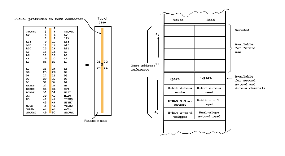
Fig.4 (right). Port address map: assignments for the interface have been chosen in consultation with Amstrad.
Scientific interface for the Amstrad PCWThe Amstrad PCW8256/8512 is marketed as a low-cost
BRIAN J. FROST
|
IC201 and IC202
(Fig.2, April issue, page 455)
which provide a separate read and write select line for each of the four ports on the card.
Port addresses and their hardware assignments (Fig.4) have been chosen in consultation with
Amstrad to ensure future upgrade capability.
 |
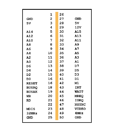
| Fig.3. Details of the Amstrad PCW connector.1 Fig.4 (right). Port address map: assignments for the interface have been chosen in consultation with Amstrad. |
|---|
IC203, a monostable which drives an 'access' led.
This has proved useful during the construction of both hardware.
Data bus transceiver IC207 is enabled by any card access and provides additional protection and fanout.
IC401 latches data written to port address A1.
The data output is displayed on leds but no attempt has been made to add extra output buffering.
This is the only external connection to the interface where protection is not available since it adds
significant complexity if speed or other compromises are to be avoided.
Data written to this address remains latched until changed.
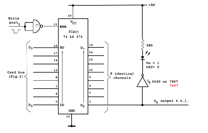 |
| Fig.5. Eight-bit t.t.l.-level output. Further buffering may be needed. |
|---|
R501 and the Schmitt triggers are fed via R502.
This arrangement is highly recommended since it provides very low loading and can be connected directly
to 15V c-mos or arbitrary logic levels, so long as the threshold of around 2V is accommodated.
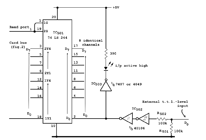 |
| Fig.6. Eight-bit t.t.l.-level input: loading of the external circuit is very low. |
|---|
R502, but this is small compared with the obtainable processor i/o
rate of around 20μs.
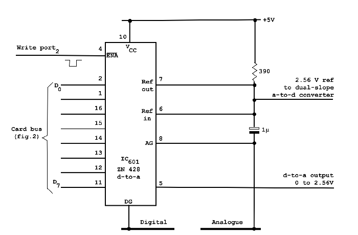 |
| Fig.7. Digital-to-analogue converter: applications include waveform synthesis. |
|---|
A2 and provides
an output voltage controlled from zero to its 2.55V internal reference.
This is fed to the optional circuitry of Fig.10 which provides scale and offset adjustment
as well as i/o protection.
IC701 with its sample
and hold buffer amplifier.
A minimum system would comprise the address decoding (Fig.2), the d.a.c. (Fig.7), a simple inverter
to derive a negative supply and this circuit to provide almost all of the waveform recording,
replay and plotting facilities.
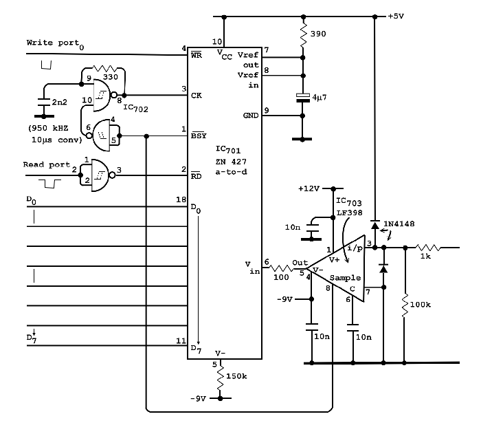 |
| Fig.8. Successive approximation a-to-d converter: conversion rate is set by the clock generator to about 100k samples per second. |
|---|
IC702 to around 10μs (100k samples per second).
During conversion the Busy output is used to force a Hold condition on IC703 to ensure no input change.
This allows the fastest sampling of dynamic waveforms without external filtering.
A0.
Internal circuitry then performs the conversion and data is available for reading at port A2.
The fixed, short conversion time eliminates the need to take the Busy signal to the processor.
Q0-Q3 together with strobe
signals DS0-DS3 which identify their significance.
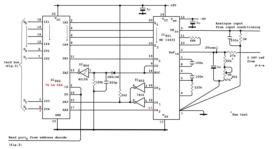 |
Fig.9 (above). For more precise measurements, the interface includes this eight-bit dual-slope converter. IC802 is an LS244. |
|---|
VR801.
The adjustment is only needed if the analogue signal conditioning is omitted, since a variable gain factor
is inherent in that section.
In this case VR801 can be replaced by a link, and 100kΩ fitted instead of the 82kΩ shown.
IC802 (timing diagram Fig. 10).
EOC which is stretched by IC804 to
ensure its visibility to the processor read loop.
The processor then loops waiting for the first strobe (DS0) to read the most significant b.c.d. digit,
followed by strobes for the other three digits.
Strobes DS1 and DS3 are combined since there is no timing ambiguity.
|
SIGNAL CONDITIONING |
IC801 (not shown) buffers and conditions
the analogue signals both inward and outward.
The circuits allow a scale factor to be set from around 0.5 to 5 times gain,
together with an offset adjustment to suit either bipolar or unipolar levels.
S101 allows a.c. coupling if required.
|
TESTING |
PORT.
This asks for the selection of a read-data or write-data fast software loop,
allowing an ordinary oscilloscope to be triggered from TP201
(the card enable line) and so probe any address or data line.
TP201.
In this case, trigger the 'scope from IOREQ (i/o request) using the PORT program and examine
the inputs and outputs of the address decoders to establish why the required port address
is not being correctly decoded.
On the prototype the +5V rail takes around 200mA and the +12V a few mA.
SIN.
|
AVOIDING PROBLEMS |
| COMPONENTS |
|
The interface is available fully assembled and tested at £139, or in the following kit stages:
Kit A: printed circuit board with connector for address decoding circuitry of Fig.2, £16.50. Kit B: address decoding circuitry of Fig.2 including p.c.b, connector, and all components fully assembled and tested, £31.50. Kit C: complete interface including case, p.c.bs, components, connectors, switches and interconnecting cable, £117,50.
Prices include postage and packing but please add v.a.t at 15%.
Orders or enquiries should be addressed to Placepower Ltd, Unit 24, Longs Industrial Estate, Englands Lane,
Gorleston, Norfolk NR31 6BE, telephone 0493 603771.
|
|
Software
For handling low-frequency waveforms, or where numerical power is required,
the interface may be controlled quite satisfactorily from the Basic supplied by Amstrad.
But to exploit the unit's highspeed waveform-handling capabilities, additional software is needed.
A suite of software is available from the author (details below):
it includes both low-level drivers and high-level programs.
If this software is to be used without modification, do not change either the port addresses
shown in Table 1 or the layout of the dual-slope a-to-d result word in Fig.10.
The driver routines help in the construction and testing of the interface and allow its operation from
Basic or from assembler:
PORT.com is intended for testing:
it allows data and decoded port addresses to be triggered or viewed on an oscilloscope.
SIN.com provides screen and keyboard control ot all interface functions.
The d-to-a converter and t.t.l. output can both be set to a specified hex value.
[It requires the system file SYSROT]
DRV.bas is for communicating with all interface functions from Basic.
This program contains source code that is merged into the user's Basic program.
[It requires the driver DRV.COM]
AD.asm is an 8080 source-code file which allows users of the CP/M MAC assembler to construct
machine-code software for their own applications.
This program performs a single read of the dual-slope a-to-d coriverter and stores the result in memory.
High-level capabilities of the suite are centred on the dedicated assembler program
WORD
(for waveform output, recording and display).
[It requires the system files SYSROT and GSX. A description of WORD will be found here]
It provides extensive facilities for waveform capture, generation and display as follows:
Recording: any waveform can be recorded via the eight-bit a-to-d converter at rates from 50μs to 50s per sample
and for a run of over 50 000 samples.
This feature turns an ordinary oscilloscope into a digital-storage oscilloscope suitable for
capturing one-off events.
It is quite adequate for digitizing speech and music.
At the start of a recording run, a positive-going t.t.l. edge is available at the digital outputs.
This has been used to stimulate external component networks and hence to display their transient response.
Replay: stored data can be replayed out through the d-to-a converter at rates from 5μs to 50s per sample,
allowing a recorded waveform to be replayed in either a looping or one-shot mode.
Data can be a previously recorded waveform, (unmodified or modified) or numerically generated
data synthesizing sine, cosine, exponential or userdefined functions.
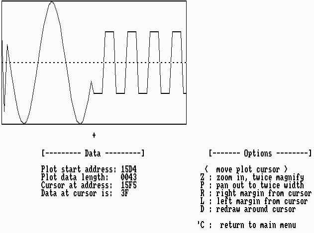
Plotting: data stored in memory can be examined on the graphics screen and plotted on the printer.
The display can be zoomed, panned and measurements made with a cursor on addresses or data.
File handling: stored data can be interchanged between memory and 'waveform' files.
These files can then contain pre-recorded waveform data as well as allowing a waveform
synthesis program to create whatever shape or function is needed and add it to the library of files.
Waveform synthesis: using simply the address decoding and d-to-a circuitry, this feature gives the
user a powerful waveform synthesizer.
A Basic program
GEN.bas allows numerical synthesis and graphical display of waveform functions such as
sine, cosine, random, pulse, with exponential envelope conditioning and user-defined shapes.
All functions can be assigned as absolute data or combined with existing data to add, multiply,
subtract and divide, allowing distortion synthesis, noise injection and modulation.
[A description of GEN.bas will be found here]
Data from this program can be read into the main
WORD program and played out at whatever timebase setting is required.
Driver and test routines for the interface can be supplied by the author in full source and object
code on CF2 disc for £8.50, or for £3.50 if you provide a blank disc.
The full program suite, which includes source and object code fully commented and with instructions, costs £17.50
(or £12.50 if you provide the disc).
Prices include postage and packing.
The author's address is 'Coppins', 8 Robinswood Drive, Ferndown, Dorset BH22 9RZ; telephone 0202-875743.
Please include a stamped, self-addressed envelope with any queries.
For readers wishing to use the CP/M editor and assembler provided by Amstrad, the 8080 source code AD.asm
is available as a listing from the Electronics & Wireless World editorial office at Quadrant House.
Send a Iarge stamped, self-addressed envelope, marking the covering envelope 'Amstrad Interface'.
|
 |
| 1. |
In Germany the PCW was supplied with another type of connector.
The connector had the same signals on the same pins.
But the numbering was different compared to the English version.
|
|